|
Liandian and Intel will collaborate on a 12 nanometer process, expected to start production in 2027Time:2024-01-29 Both parties will provide EDA and IP solutions through ecosystem partners to support the design and implementation of the 12 nanometer process. It is expected that this 12 nanometer process will be put into production in 2027.
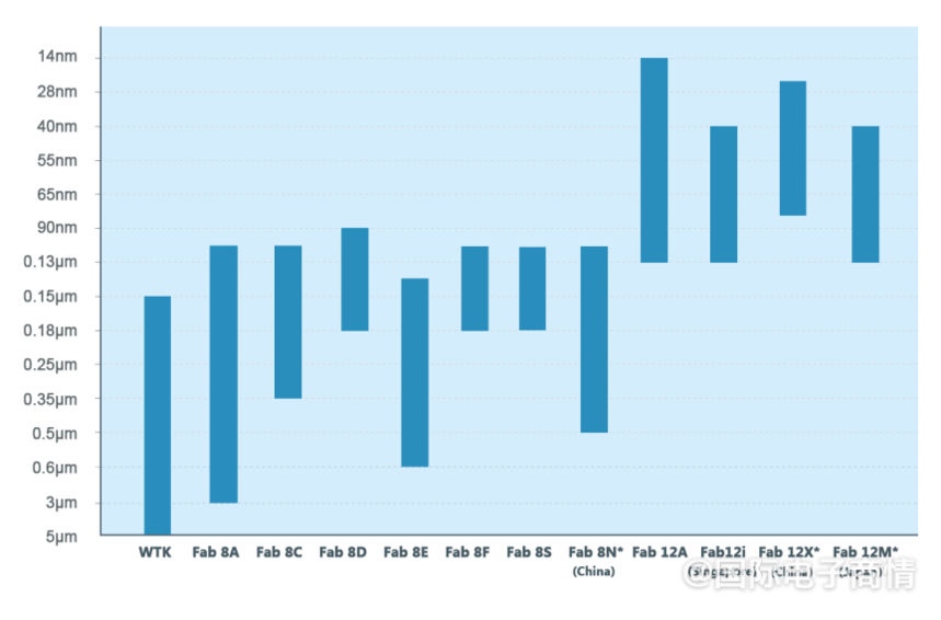
Various process technologies of Liandian (official information) Stuart Pann, Senior Vice President and General Manager of wafer foundry services (IFS) at Intel, said, "Intel's strategic partnership with Unilever further fulfills its commitment to providing technology and manufacturing innovation for the global semiconductor supply chain, and is an important step towards achieving Intel's goal of becoming the world's second largest wafer foundry by 2030." According to data, Intel has invested and innovated in the United States and globally for over 55 years. In addition to Ireland, Germany, Poland, Israel, and Malaysia, it has also established or planned manufacturing bases in Oregon, Colombia, New Mexico, and Ohio in the United States, as well as invested in wafer foundry services (IFS). Significant progress has been made in 2023, including new customers adopting Intel 16, Intel 3, and Intel 18A process technologies. Intel divests a large number of non core businessesIn July 2023, Intel announced its withdrawal from its NUC mini PC business and licensed the NUC design to computer manufacturer Asus. In September, Intel announced that it had agreed to sell approximately 10% of IMS shares to TSMC. TSMC's investment in IMS is valued at approximately $4.3 billion this time. Intel will retain a majority stake in IMS, while IMS will continue to operate as an independent subsidiary of the former and under the leadership of its CEO Elmar Platzgummer. IMS, also known as IMS Nanofabrication Global, LLC, is a subsidiary of Intel Holdings. Since the invention of multi beam technology and the launch of the first commercial multi beam mask writer in 2015, IMS, headquartered in Vienna, Austria, has been an industry leader in the field of advanced technology node multi beam mask writing. In October, Intel announced its intention to separate its Programmable Solutions Division (PSG) business into a separate business. Intel expects to report on PSG as an independent business unit when releasing its Q1 2024 financial report. In the next two to three years, Intel plans to conduct an initial public offering for PSG and may explore opportunities with private investors to accelerate the growth of the business, while retaining a majority stake. At that time, the two companies will continue to maintain strategic cooperation, including PSG continuing to cooperate with Intel wafer foundry services (IFS). In November, it is rumored that Intel plans to transfer its silicon optical module business to electronic manufacturing services company Jabil. This is one of Intel's strategies to continue divesting non core businesses. Previously, Intel Mobileye's business successfully completed its IPO in 2022. In summary, these transactions highlight Intel's high focus on advancing its IDM 2.0 strategy. |


